Video presentation
Around 80 % of the CO2 footprint of average electronic components is already caused during production. Ein Forschungsteam des Fraunhofer EMFT arbeitet daran, Prozesse in der Halbleiterfertigung zu optimieren, um den Einsatz klimaschädlicher Prozessgase zu minimieren. In the process, the scientists are also testing more climate-friendly alternatives to etching gases that have been used as standard to date.
An article by Robert Wieland
Fraunhofer Institute for Electronic Microsystems and Solid State Technologies EMFT
Electronic products carry an ecological backpack - that's common knowledge today. What may come as a surprise, however, is that the lion's share of a product's CO2 emissions, around 80%, does not come from usage but from production.
Why is that?
The example of semiconductor manufacturing impressively demonstrates this. Deep etching is a critical basic process in this area for introducing microstructures into a silicon wafer. Until now, the highly climate-damaging gas sulfur hexafluoride (SF6) has been used for this purpose - one of the main reasons for the poor eco-balance.
A research team from Fraunhofer Institute for Electronic Microsystems and Solid State Technologies EMFT addresses this point: They aim to reduce the amount of process media required by optimizing the technology process. They are also working on alternatives to the harmful fluorine gas. As part of the BMBF project SUMSi, the team is developing two novel plasma sources for deep silicon etching that allow significantly smaller process chambers: a so-called INCA source - an inductively coupled plasma array - and a microwave-activated, planar plasma rod source.
The developments focus on an efficient, area-scalable plasma source concept, rapid gas exchange when switching between the passivation step and the etching step, lower process gas consumption due to a better degree of decomposition of the process gases and, as a result, a lower waste gas load that is harmful to the climate.
Both versions have already been successfully tested in the plasma etching chamber at Fraunhofer EMFT in the so-called "Bosch process" during the development period of just 11 months. The process is based on regular alternation between passivation and Si-etching and is used as standard in industrial production to manufacture microstructures.
The scientists used three different process media: C4F8 (passivation gas), SF6 (climate-damaging etching gas), and a FAN gas mixture (climate-friendly etching gas, mixture of F2/Ar/N2). The etch rates - i.e., the material erosion per time - were comparable or even higher with SF6 than with currently used systems. The more climate-friendly alternatives are presently lower due to the significantly lower fluorine content. Given the enormous CO2 savings potential, there is no doubt that the research team will continue to work on this topic:
A first estimate for the CO2 equivalent of the Bosch process with SF6 for Si depth etchings results in about 6,500t CO2-eq emissions for the operation of a smaller MEMS fab. By comparison, using alternative, more climate-friendly gases would reduce CO2 eq by more than a factor of 10 to about 530t CO2 -eq. Therefore, the search for more environmentally friendly process solutions has only just begun and is being intensively pursued at Fraunhofer EMFT as part of the Green ICT initiative.
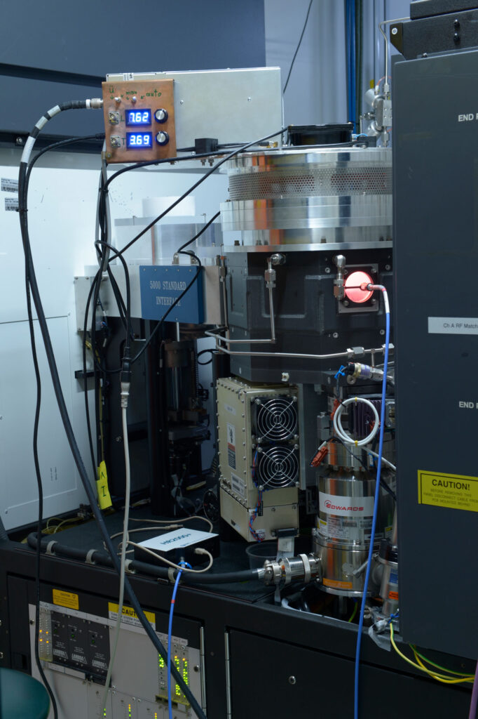
INCA plasma source (Inductive Coupled Array) with ignited plasma - fluorine gas mixture instead of SF6. The newly developed INCA plasma source consists of the upper part (bare Al), including an automatic matching unit, and was adapted to an already existing plasma etching chamber at Fraunhofer EMFT. The pink color typical for N2 (nitrogen) results from the N2 contained in the fluorine gas mixture.