A project of the start-up DIVE imaging systems GmbH
Ecological savings in semiconductor production
The project idea aims to quantify the ecological savings in semiconductor production with the help of hyperspectral vision technology. By using this screening tool, system control wafers can be saved, production errors avoided, and production capacities used in a more resource-efficient manner.
DIVE imaging systems GmbH develops innovative inspection tools that combine the advantages of optical spectroscopy with imaging. AI algorithms make the process steps in semiconductor production more comprehensively controllable, and the use of operating resources can be reduced.
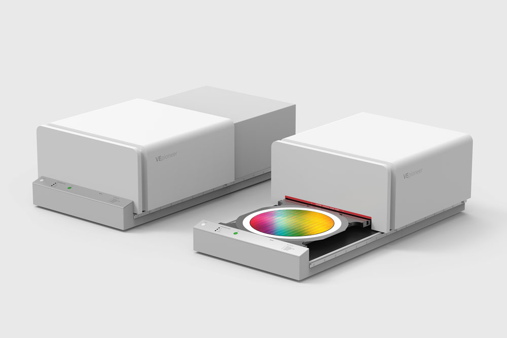
Wafer measurements in seconds
The ecological savings potential is quantified in two steps in the Green ICT Space project. First, the VEpioneer system is qualified for cleanroom use, followed by implementing a further developed system solution for 100% control of the production steps.
DIVE's technology enables more efficient process monitoring and control in resource-intensive semiconductor production. Wafer measurements can be carried out in a matter of seconds.
Considerable resource savings expected
Early fault detection can save resources and reduce faulty production, which leads to a reduction in CO2 emissions, water consumption and process chemicals. Potential savings of up to 40% are possible in front-end production. The exact savings potential for each process step will be quantified over the course of the project.
Commercial distribution and further development of the developed system solution
Once the project has been completed, the system solutions developed for the cleanroom will be actively marketed to customers in semiconductor production. The plan is to develop the technology further and establish a joint test bed for potential users from industry and science.
Project partner:
Dr. Philipp Wollmann, Dr. Wulf Grählert, DIVE imaging systems GmbH
Fraunhofer Institute for Photonic Microsystems IPMS
Project period:
Start: January 1, 2024, end: December 31, 2024