The sustainability check for your processes in microelectronics production

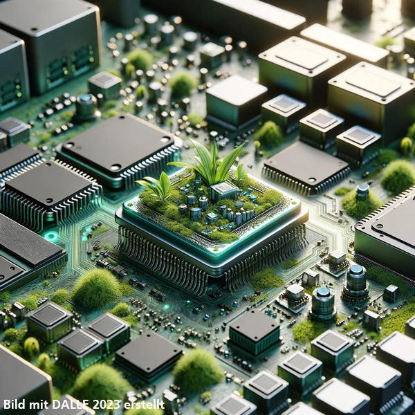
Services from Hub III: Resource-optimized electronics production

We examine your microelectronics production and develop proposals to reduce your CO2e footprint. Apply for a validation project and have your innovative manufacturing process checked right through to the product free of charge!

Areas examined: 

  • Resource-optimized microelectronic processes 
  • Energy-efficient cleanroom environment 
  • Decrease of harmful exhaust emissions 
  • Optimization of individual processes in terms of energy and material consumption 
  • Sustainable design and connection technology 
  • Replacement of critical materials (CMR and/or PFAS materials) 

Focus topics: 

  • Consideration in operation: energy savings in selected scenarios 
  • Consideration of the resource input during production by determining the CO2e footprint (if information is available for the calculation or assessment).
  • We offer to carry out a life cycle assessment for your manufacturing processes.
  • The validation project's result is presented as a case study (theoretical consideration), which illustrates the savings potential through Green ICT technology. The final results are also published. Company-specific data will be treated confidentially on request.

What we offer

Reconditioning of carrier wafers
More info
  • Cleaning process for 300mm glass wafers for multiple reuse of glass wafers
  • Reduction of glass wafer scrap and thus of CO2-Emmissionen
New cleaning methods in wet chemistry
More info

  • EKC265 substitution for cleaning TSV according to Bosch process
  • Use of solvents or solvent mixtures that are not carcinogenic and not very harmful to aquatic organisms
FEOL Thermal processing
More info
  • Replacement of traditional batch furnace processes by rapid thermal processing in the field of high-quality oxides (e.g. gate oxidation) for the production of complex technologies
  • Evaluation of material and energy consumption for technology modules using furnace oxides
Metal-metal bonding processes
More info
  • Use of hybrid integration based on Al-Al wafer bonding in the MPW range, production of hybrid technologies with optimized performance-cost-trade-off
  • Evaluation of material and energy consumption for entire technology processes in terms of consumption vs. expenditure

EKC replacement for post-metal etch remover
More info
  • Introduction of more environmentally friendly alternatives than EKC265 for cleaning
  • Fluorides, amines, hydroxylamine and pyrocatechol-free, low process temperature, without rinsing with isopropanol
Optimization of consumption CMP
More info
  • Process optimization with slurries from less critical sources or materials, advice on recycling tools, characterization on test structures
  • Replacement of Ce- by SiO2-containing slurries; reduction of water consumption in the post-process, recycling and re-use of slurries, determination of consumption and CO2-equivalents
Footprint creation in photolithography
More info
  • Creation of the IN/OUT material and energy flows of a coater and developer in an industrial environment
  • Process-dependent CO2-balancing and optimization

PECVD Clean mit Fluorgasmischung (FAN = F<sub>2</sub>/Ar/N<sub>2</sub>)
More info
  • Advice on FAN gas installation, creation and optimization of the plasma cleaning recipe
  • Complete replacement of climate-damaging cleaning gases (C2F6 und NF3) through FAN gas
Integrated scrubber system incl. analysis and treatment of harmful gases
More info
  • Harmful gases, investigation of PECVD cleaning processes. Available cleaning gases: PFCs, SF6, NF3, FAN
  • Processes with the lowest possible amount of wash water or lowest possible propane gas flow

Energy management
More info
  • Balancing of processes that are linked to energy quantities, including optimization
  • Life cycle assessment of specific oxides possible

Optimizing the media savings of tools in semiconductor production
More info
  • Consulting on energy efficiency when using machines and systems. With mobile energy loggers, the electrical parameters can be recorded with time resolution and correlated directly with running processes
  • Depending on the initial situation, tool-dependent energy savings of up to 25 % can be achieved. Measurements allow life cycle assessment of individual processes

Replacement materials & optimized packaging processes
More info
  • Process parameters for the production of InGaAs/InAlAs/InP heterostructures on silicon substrates
  • Reduction of the arsenic content in electronic high-frequency circuits by 99.99 %

NMP replacement
More info
  • Alternative NMP substances with advantages and disadvantages have been tested. These tests can be extended by extensive knowledge of characterizations.
  • Process evaluation without NMP

Application form

    Company name and address

    Company website

    Contact person

    Contact person email

    Contact person phone number

    Please describe in a few words what makes your solution special.

    To which subject area of resource-optimized electronics production would you assign your inquiry? (multiple answers possible)

    ProcessingCleanroom and infrastructureEnergy management in production linesStructure and connection technologyMaterial replacementHolistic accounting

    Would you like to use our equipment park for your proposal?

    YesNo, implementation should take place in the company's own environment

    Can you already name the fields of application that you are addressing with your solution?

    How did you hear about our offer?

    RecommendationOwn research

    Would you like to subscribe to our newsletter? (in German)

    YesNo