The aim of the Green ICT Space project "New Screening Tool for Efficient Semiconductor Manufacturing" (NEST) was to quantify potential environmental savings in semiconductor manufacturing using hyperspectral vision technology while at the same time supporting the young start-up in introducing the new measurement method in commercial semiconductor fabs and foundries.
DIVE imaging systems GmbH develops innovative inspection tools that combine the advantages of optical spectroscopy with image capture. AI algorithms make the process steps in semiconductor manufacturing more comprehensively controllable, which can reduce the use of operating resources as well as the number of control wafers.
The non-destructive and high-precision inspection technology can be used for quality control of wafers and leads to a saving of control wafers. These are introduced into the production process in addition to the actual production wafers in order to check the quality of individual process steps.
As part of the environmental potential analysis, the advantages of using DIVE technology were compared with the state of the art, with a particular focus on the energy input per wafer. For an exemplary 28 nm process (CMOS, front-end), around 700 process steps were assumed for production, including approx. 400 process steps for wafer processing (etching, lithography, deposition) and approx. 300 accompanying metrology process steps.
For the 28 nm production process, the use of 36k control wafers was assumed for 25k wafer starts/month, and the savings potential achievable through DIVE technology was initially conservatively estimated at 25% of the control wafers (9,000 wafers/month). Based on these assumptions for a 28 nm process, Fraunhofer IZM developed a simplified process flow model based on literature data. The model takes into account the type and number of key process steps. Based on a defined energy mix, in this case 600 gCO2e/kWh, the CO2footprint of production was calculated in kgCO2e before and after savings.
By using DIVE's hyperspectral vision technology, more than 118,000 kilograms of CO2 can be saved every month. The reduction in the CO2footprint takes into account additional energy costs for the manufacture and operation of the DIVE system. This corresponds to a reduction of around 2% of the monthly Fab CO2footprint. Other positive effects were explicitly not included in the calculation:
- Early detection of process deviations and thus savings on production errors and positive influence on the yield of the production wafers
- Reduction of tool allocation through control wafers or saving on the operation of dedicated tools that are used exclusively for processing control wafers
- Energy savings resulting from the elimination of the processing steps for control wafers
- Reduction in the consumption of chemicals and water required for the preparation of control wafers, in particular the use of concentrated mineral acids
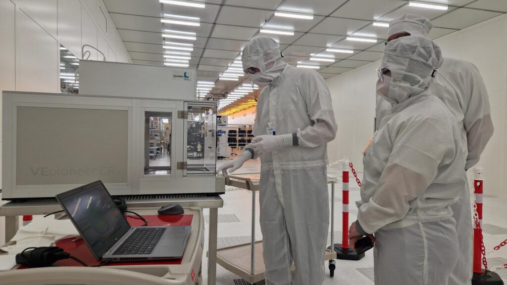
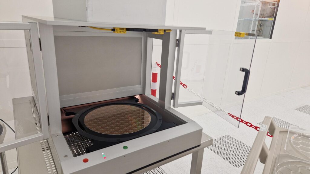
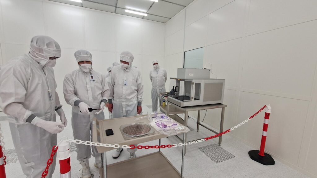
In addition to the environmental potential analysis, the cooperation within the Green ICT Space project has contributed significantly to DIVE's ability to address the market for cleanroom-compatible measuring devices for semiconductor fabs. In the course of the project, an initial cleanroom-compatible measuring device was set up in the 300 mm cleanroom at Fraunhofer IPMS with the support of Fraunhofer IPMS.
The plan is to continue using the cleanroom-compatible DIVE VEpioneer® system at Fraunhofer IPMS after the project ends on June 30, 2025. This will allow the startup to continue evaluating the system on site with customers from the semiconductor industry and performing wafer measurements for customers under cleanroom conditions. In the future, the system will be further developed with automated wafer handling and equipment coupling for automatic data transfer. Follow-up projects between DIVE and Fraunhofer IPMS are currently in preparation.
In May 2025, it was announced that DIVE Imaging Systems GmbH had been acquired by PVA TePla AG. PVA TePla is a leading high-tech company specializing in material and measurement technology. Founded in 1991, the system provider develops and manufactures customized solutions for high-precision material manufacturing, finishing, and processing (Material Solutions) as well as systems for inspecting materials and components using acoustic, wet chemical, and optical methods (Metrology). With its Technology Hub, PVA TePla operates an innovation center for market-oriented research and development of materials of the future. In addition, the company's internal research and development department also serves highly specific individual customer requirements.
The Green ICT Space project NEST, with its practical focus on the semiconductor industry, has played a key role in helping DIVE take a decisive step toward establishing itself on the market with its innovative measurement method.