A contribution by Quoc Hung Nguyen, Karl Neumeier (Fraunhofer EMFT), Jenichi Clarivaux Felizco and David Sánchez (Fraunhofer IZM)
In semiconductor manufacturing, dry etching for structuring conducting lines and interconnects (VIAs) generates unwanted residual polymers that can cause serious device reliability problems. Instead of the usual cleaning chemicals, which are often harmful to the environment, Fraunhofer EMFT has successfully implemented a significantly sustainable process. According to a simplified life cycle assessment by Fraunhofer IZM, this would reduce CO₂ emissions by around 42%.
Back-end-of-line (BEOL) processes create the necessary electrical connections between the active and passive components manufactured in the front-end-of-line (FEOL) and the external connections. The metal layers are usually deposited using sputtering processes. These metal layers are usually separated from each other by silicon dioxide layers, which are formed using low-temperature Chemical Vapor Deposition (CVD) processes. Both layers are structured to create the conducting lines and VIAs using dry etching processes. Multiple wiring levels are often necessary to achieve crossing-free routing and short wiring paths.
Dry etching processes are characterized by steep etch sidewalls. This is achieved by in situ passivation of the freshly created etch-slopes with polymers, which are usually fluorocarbon compounds (CXFY). The “precursors” can come from the etching gas mixture and/or the photoresist used for masking. These polymers can be removed by ashing in oxygen plasma.
During metal and VIA etching, these polymers are modified by metal ions or radicals that are produced during the etching process in such a way that they cannot be adequately removed by ashing. If these polymer residues are not removed, the undesirable topography and any remaining polymer residues can lead to increased contact resistance and/or increased electromigration, resulting in serious reliability problems.
Environmentally harmful and toxic chemicals in conventional cleaning processes
Polymer residues are typically removed through a dual cleaning process: plasma stripping and a wet process. The solutions for wet process used in industry usually contain toxic or environmentally harmful chemicals such as N-methyl-2-pyrrolidinone (NMP), tetramethylammonium hydroxide (TMAH), pyrocatechol, or hydroxylamine. For technologies that use aluminum as a wiring level, EKC265 (DuPont EKC Technology) is often used as a highly selective post-metal and via etch residue remover. In industry and at the Fraunhofer Institute for Electronic Microsystems and Solid State Technologies (EMFT), EKC265 has been used successfully for more than 20 years to clean residues after metal and VIA plasma etching. This EKC265 mixture consists of diglycolamine, hydroxylamine, and pyrocatechol. The latter two substances are classified as carcinogens. In addition, hydroxylamine is very easily absorbed through the skin and is very toxic/harmful to aquatic organisms. Together with water, diglycolamine forms an alkaline solution that can attack both silicon and aluminum, which is why two isopropanol rinsing sequences are necessary before water rinsing.
Alternative process is more environmentally friendly and faster
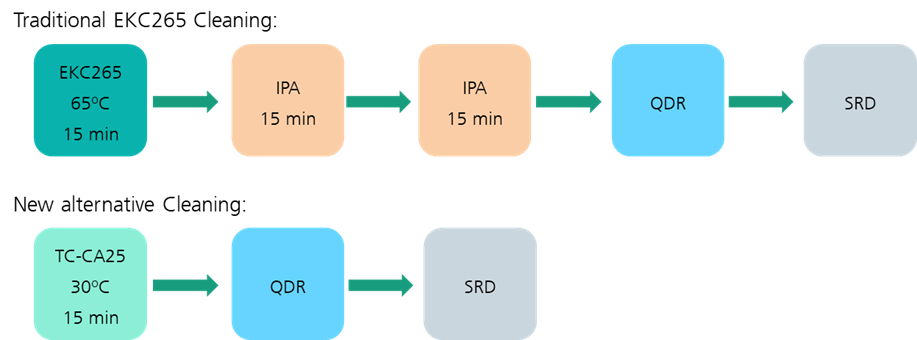
As part of the “Green ICT @ FMD” project, a research team at Fraunhofer EMFT has successfully tested a new alternative mixture for removing etching polymers after plasma etching of metal structures on wafers. The new mixture has a low environmental impact as it is based on a semi-aqueous solution of polycarboxylic acids that contains neither fluorides, amines, hydroxylamine, or pyrocatechol. In addition, our initial results have shown that the new cleaning process does not require the two intermediate steps of rinsing the wafers with isopropanol, as is the case with EKC265 cleaning for the reasons mentioned above. This results in a significant reduction in process time of 30 minutes, compared with 70 minutes total of total process time in previous process. Fig. 1 shows a comparison between the two cleaning processes. Each cleaning process involved 25 wafers (batch process) with a wafer size of 150 mm and 200 mm in diameter.
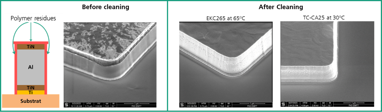
Comparisons between the cleaning with EKC265 and with the new mixture were carried out after TiN/AlSi/TiN/Ti layers (800 nm) on Si wafers coated with 500 nm SiO2 were structured by plasma dry etching. After plasma etching and in-situ resist stripping, polymer layers form on the surface and side walls of the metal layers (Fig. 2, left). Cleaning with TC-CA25 at 30°C resulted in clean metal layers, as the polymer residues were completely removed (Fig. 2, right). The results showed that the cleaning quality of the new alternative is the same as that of EKC265.
Life cycle assessment of the new cleaning process
To evaluate the environmental impact of the two processes, Fraunhofer IZM performed a simplified CO2assessment. For the comparison, the functional unit for cleaning was defined as a batch of 25 200-mm wafers. The analysis takes into account both the energy consumption during the cleaning process (mainly to achieve the desired cleaning temperature) and the chemicals required in both processes (the components of both cleaning mixtures as well as isopropanol and water).
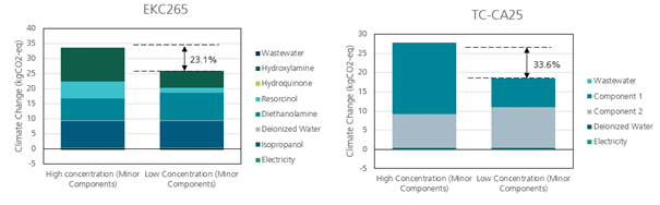
The results of the CO2 footprint analysis for both processes are shown in Fig. 3. Since the exact concentrations of the individual components in commercial mixtures are unknown, the result varies depending on the concentrations used in the calculation. Overall, the TC-CA25 process has lower total emissions than the EKC-265 process, with a potential reduction in CO2 emissions of approximately 42%. In addition, the TC-CA25 process saves additional resources for the treatment of chemical waste due to its lower chemical consumption.
The newly established cleaning process developed by Fraunhofer EMFT for removal of polymer residues after metal and via etching not only demonstrates the same cleaning efficiency as the conventional product but also has a lower environmental impact. The experience gained and this expertise are now available to interested partners from industry and business.
The Green ICT Competence Center at the Research Fab Microelectronics Germany (“Green ICT @ FMD”) is a central point of contact for sustainable electronics. The German Federal Ministry of Education and Research supports the project as part of the Green ICT initiative, which is part of the German government's 2030 climate protection program. Fraunhofer IZM and Fraunhofer EMFT are part of the competence center.